
Members:
Mustafa Al Momin
Christian Brown
Advisor: Dr. Ross Snider
Sponsor: Resonon Inc.
I. Introduction:
Resonon, Inc. currently uses a computer system to analyze data input from a hyperspectral imager. A hyperspectral imager collects spectraal images that provide far more color (spectral) data per pixel than conventional color cameras. We would like to design a FPGA which could be used to both capture the data and analyze it. Project Tasks Time 1. Learn how the hyperspectral imager works (i.e. gathers data, what the data means, and how it outputs it) and determine the exact requirements of the project. 6 weeks 2. Design C program in Linux environment on the FPGA to take data input stream from gigabit-Ethernet, format it and store it in an sd card. 10 weeks 3. Design vhdl code to stream the data to dram in the fabric and then output to HDMI to show grayscale image of the 2d matrix. (Completed concurrently with 2. by a second team member.) 10 weeks Costs: ~$0 because Ross Snider will be supplying what we need.
II.Problem Statement:
The existing hyperspectral imager uses a computer for data acquisition and analysis, which is costly and slow to operate (in comparison to an FPGA). The purpose of this project is to design an FPGA utilizing a hyperspectral imager for image acquisition and pixel classification using a machine vision algorithm. Image acquisition will occur through a gigabit Ethernet port.
Scope/Bounds:
1. The clock speed of FPGA is relatively slow compared to a computer. However, it can process much more data in parallel (per clock cycle) than a computer.
2. The FPGA is low cost and needs much less power than a computer to operate.
2. The number of pixels that can be acquired and/or classified in parallel at one time.
4. Data output rate of hyperspectral imaging camera.
Statement of need:
The sponsoring company uses hyperspectral imaging to classify the colors of almonds on a belt and then takes that information to operate a system which expels the bad almonds based on a specific set of criteria. Designing an FPGA which acquires and analyzes the data (especially with the possibility of using an ARM core as on the Cyclone V), the belt could be sped up considerably and therefore save plenty of time. (Ex: 4Ghz comp with at most 10 inner product engines in parallel vs. 100Mhz clock with up to 4000 inner product engines running in parallel is equivalent to a speed boost of ~10000%)
Level One Requirements (sponsor-approved deliverables):
SoftwareMove data to HPS SDRAM
1. Camera Specification: Mako G-032 (12 bit depth at 102 frames/sec with 658 x 492 resolution (maximum output) which converts to 49.531608MB/sec)
2. Gigabit Ethernet interface from camera to FPGA (max data rate of 125MB/sec)
3. Software to get data to buffer in SDRAM
Hardware
Implement VHDL components to move data from DRAM to Monitor
1. DMA controller to move data from HPS SDRAM to FPGA SDRAM
2. HDMI controller to output data from FPGA SDRAM to HDMI Monitor
Needs:
1. A hyperspectral imager and or a similar system which outputs data at a similar speed through a gigabit Ethernet port the same way that a hyperspectral imager outputs data.
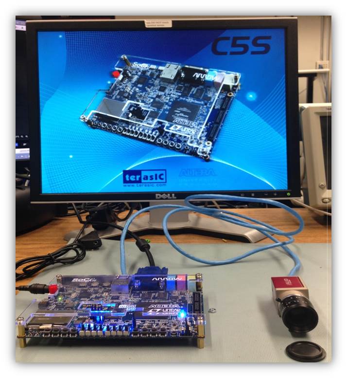
2. An FPGA development board and kit which has the necessary ports for a gigabit Ethernet and HDMI output.
III. Background Problem definition:
Our system collects and processes information from across the electromagnetic spectrum. FPGAs serve as “glue logic” between off the shelf components, and as replacements for ASICs in first generation products. Recently, however, FPGAs have become so dense and fast that they have evolved into the central processors of powerful reconfigurable computing systems [1]. A Xilinx XCV-2000E, for example, contains 38,400 logic blocks, and can operate at speeds of up to 180MHz. The logic blocks can be configured so as to exploit data, pipeline, process, or I/O parallelism, or all of the above. In computer vision and image processing, FPGAs have already been used to accelerate real-time point tracking, stereo , color-based object detection [4], and video and image compression.
Altera FPGA:
Digital camera resolution: 4096 x 1714 pixels. Structured ASIC migration path to low costs: Altera structured ASICs start at US$15 at 100ku for 1 million ASIC gates. Altera's Video and Image Processing Solution: This includes optimized DSP Design Flows, Altera's Video and Image Processing Suite, and interface and third-party video compression IP, and video reference designs.
In image processing, FPGAs have shown very high performance in spite of their low operational frequency. This high performance comes from
(1) high parallelism in applications in image processing,
(2) high ratio of 8 bit operations, and
(3) a large number of internal memory banks on FPGAs which can be accessed in parallel. In the recent microprocessors, it becomes possible to execute SIMD instructions on 128 bit data in one clock cycle. Furthermore, these processors support multi-cores and large cache memory which can hold all image data for each core.
The performance of FPGAs with those processors using three applications in image processing, the three being two-dimensional filters, stereo-vision and k-means clustering, makes it clear how fast an FPGA processes an image, and how many hardware resources are required to achieve the performance.
The economics of FPGAs are fundamentally different from the economics of other parallel architectures. Because of the comparatively small size of the image processing market, most special-purpose image processors have been unable to keep pace with advances in general purpose processors. As a result, researchers who adopt them are often left with obsolete technology. FPGAs, on the other hand, enjoy a multi-billion dollar market as low-cost ASIC replacements. Consequently, increases in FPGA speeds and capacities have followed or exceeded Moore’s law for the last several years, and researchers can continue to expect them to keep pace with general-purpose processors.
This entire project is expected to be built in VHDL and so it will follow the IEEE Standard VHDL Language as specified in their reference manual.[5]
It is possible that a camera-link interface may have to be used and/or the entire interface designed by our team for this project. However, in our 2nd meeting with the project advisor this was made null. Since this is a rough draft, we’re linking a webpage to an explanation of the camera-link interface standard specifications. [6]
As far as a link to the hyperspectral imager through gigabit Ethernet which, Altera offers pre-made designs for implementation with their FPGAs. Gigabit Ethernet is a cost-effective technology when used to do the following: Connect multiple devices to a local CPU, Interconnect multiple boards across a backplane or across systems for data transfer, and Control signaling between line cards and the host CPU within an embedded system.
IV. Design Specifications Interface Specifications:
The C program will tell the fabric when to store data and when to multiply the pixel data vectors with the classification vector. The fabric will only allow the C program to input information and write to a bit telling the fabric to “go” and store information and/or multiply the vectors. The output will be read only by the C program. The classification vector will be preloaded into a register of the FPGA for fast access. Cyclone V FPGA (Due to hardware being predefined and chosen by the sponsor, no numeric specifications will be used.)
VHDL: Create a component to store and write information to RAM. Design an inner product engine which will classify each pixel by multiplying the pixel color information by a vector classification vector given to us by our sponsor. Create a top-level interface to utilize both components. Classification vector will be preloaded in memory in a register or cache.
C Programming: Create a circular buffer which will tell the FPGA to multiply the vectors together and then output the resulting information in a way such that the C program can use that information to send signals to an actuator. Design a C program in the Linux environment in Cyclone V in order to get input from gigabit Ethernet interface and store it into registers of the FPGA. Design a linker code which will introduce the “C program” with predefined color code so that “C program” can analyze the input and make decision. Another header file will be created to get the decision and store the output again to the registers of the FPGA so that VHDL can access it.
V. Design Alternatives Creation and Evaluation:
Options: One option from each numbered section must be chosen.
1a. The C program can store and multiply information in hardware with a single write to the “go” bit, or
1b. The multiplication of vectors and storing of information from Ethernet are done in separate steps.
Option 1a would be the best not considering time involved. Option 1b will be easier to debug. Additionally, option 1b would be easier to code and would be the best option to strive for at the start because it will be easy to morph into option a once it works correctly.
2a. The C program could store incoming information from the gigabit Ethernet in a circular buffer and then tell the fabric when to “go.” “Go” can mean storing information in RAM as well as multiplying the vectors together as stated in the first option. “Go” can also be used to signify that the C program is telling the fabric to store information and then waiting for a flag from the fabric to tell it that it is ready to store another vector and/or multiply vectors together, or
2b. The C program could link the output stream from the Ethernet directly to the hardware and tell the hardware when to store information simply based on busy flags.
Option 2b would be the best way to go. However, due to the design of the Cyclone V FPGA, it may be impossible to implement. Since the Cyclone V is very new and has had little experimentation done with it, it is impossible to know if option 2b is possible to do at this time and will have to be investigated further with code testing.
Depending upon the timing of option a, it may not be viable option in that it would slow down the entire system by a great amount. The whole point of designing this is to speed up the information retrieval and synthesis system. Half of the speed increase, or goal, of the project lies on this design decision. However, we cannot know for sure if option 2b is even possible until it has been coded.
3a. The VHDL code could be written such that everything is built in one VHDL file, or b. The VHDL code could be made up of a main file and several component files. The two (main) components would be receive and/or store information in RAM and multiply vectors together.
Option 3a is what the VHDL programmer has been primarily successful with in the past yet is considered poor programming practice. An experienced VHDL programmer would be able to understand, modify, and debug option 3b much easier. Design choices: Option 1b and 3b are definite. Option 2a will most likely be designed due to its simplicity. Option 2b will be explored and, if possible, will be implemented in the final design.