Device Build
The remote sensing device was built and tested in two major stages. First, only the critical componets were assembled on a breadboard while both the DC-DC boost supply and the MCU were left on their respective development boards. Here, the majority of the transient protection circuitry was left off, and the device was tested at room temperature only. The second (final) stage was testing on the Printed Circuit Board (PCB). This allowed all the miniscule Surface Mount Devices (SMD) to be tested along with sleep current.
Prototype
For the prototype build, a lab DC supply was used to power the system. In addition, Silicon Labs C8051F410 development kit was used for firmware development. The primary purpose of this build was to demonstrate basic functionality and allow for firmware development. In this build, only the Geoforce transmitter, MCU, DC-DC boost, current limiter, inductive choke, linear amplifier, and status LED were used. The additional components seen are either resistors or the I2C bus protocal sniffer. Figure 1 shows this setup.

This setup resulted in an average of 2% error from the sensor current to the value transmitted.
PCB Layout
The printed circuit board (PCB) layout was done using the Mentor Graphics PADS Logic/Layout software. Figure 2 shows the completed design including all layers. Red Represents the bottom layer, while blue represents the top.

The reason for an entire ground layer is so that for any component requiring a ground connection, it can have a ground connected next to it by dropping a via and connecting through that via to ground with the bottom layer. This helps maintain high performance since a long trace leading to ground can create unwanted resistance. However, it is fairly difficult or even impossible to trace everything on the top layer, thus some traces were outlined on the bottom layer. These bottom traces were kept minimal and as short as possible to maintain maximum performance. Furthermore, a 20 mils (~0.5 mm) clearance is made between these bottom traces and the copper (that filled the bottom ground layer) to avoid shorting.
Capacitors C5 and C7 were placed close to the input of the microcontroller so that much of the high frequencies from the power supply can be eliminated before the input. Furthermore, in the layout of the U3 (TPS61040) DC-DC boost converter, the inductor and the diode unit is placed as close as possible to the switch pin to minimize noise coupling into other circuits. Additionally, the traces for these units are large and wide pours rather than regular tracks as to avoid inductive noise.
Assembled PCB
Once received, and all components placed, the PCB worked well with a few exceptions. These issues caused the MCU to be unable to communicate with the programmer through the debug header. First, the footprint for the reset switch (SW1) was rotated 90 degrees. This was causing the reset line to be continuously pulled low holding the MCU in its reset state. Secondly, the trace connecting pin 32 of the MCU was incorrectly routed to R7 instead of R3. Finally, R3 should not have been connected to pin 6 on the debug header through one of R7's pads. These issues were fixed through carefull trace cutting and wire bridging. The corrected PCB can be seen in Figure 3.
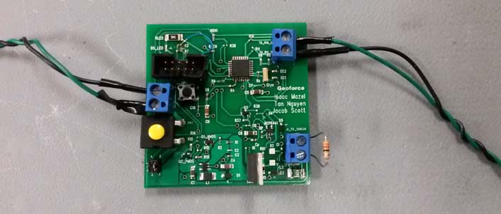
(note: wires on left and right connect to the battery pack and the MYTE transmitter respectivley)
Figure 4 shows the entire system.

(note: resistor connected across upper left screw terminal (blue) is dummy load in place of 4-20 mA loop sensor)
During test runs, a Software Defined Radio (SDR) was placed near Geoforce's antenna. Figure 5 shows the spectrum of the signal between our project and GlobalStar's satellite near 1.6 GHz. By utilizing the configuration settings only available to Geoforce, the payload transmitted was forwarded to the team via an XML encoded email. The following piece of XML shows what was received: <raw_payload>0000000000005f2000</raw_payload>. In this case, the data received was 0x5F20 which corresponds to a sensor current of 17.295 mA with no error flags.