Hardware
After weeks of preliminary design and alternatives evaluation we have decided to implement a Field Programmable Gate Array (FPGA) system with an array of six sensors to collect the data necessary for the balloon flight.
- Analog Devices ADXL345 Triple Axis Accelerometer
- InvenSense ITG-3200 Triple-Axis Digital-Output Gyro
- Freescale MAG3110 Triple Axis Magnetometer
- Bosch BMP085 Barometric Pressure Sensor
- Trimble Lassen iQ GPS Receiver
- Texas Instruments ADS1118 ADC w/ k-type thermocouple
The system will take advantage of the "System on a programmable chip" approach. Creating custom interfaces for each sensor will allow for efficient simultaneous data collect. The data will be written to a MicroSD flash card.
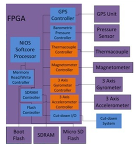
The boot flash memory will load the custom bit stream application to the FPGA during power up. The cut-down line will most likely be a transistor circuit that will allow the control of current to the cut down system (nichrome wire).
We will be able to collect GPS information at a rate of atleast 1Hz. Using the combination of gyrometer, magnetometer and accelerometer along with a dead reckoning algorithm we will be able to predict the position between GPD pulses.
The combination of GPS altitude and pressure/temperature readings will create a redundant system for the most important peice of information (the height of the ballon at each picture).
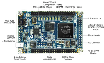
Altera's DE0-Nano education and development board offers the perfect platform for this project. It features a powerful Altera Cyclone IV FPGA (with 22,320 logic elements), 32 MB of SDRAM, 2 Kb EEPROM, and a 16 Mb serial configuration memory device.For connecting to real-world sensors the DE0-Nano includes a National Semiconductor 8-channel 12-bit A/D converter and expansion headers that can be used to attach other devices and is perfect for designing a custom PCB device. Altera also has the most comprehensive design tools on the market.
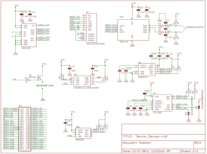
Here is a schematic layout of all of the sensors showing how they connect to the 40 pin header on the DE0-Nano board.
Software
Each sensor described will have be designed and implemented so the formatted data is available on a memory mapped register for the C code to access.
The FPGA system architecture allows each sensor to have its own set of readable registers. Once the data is written to the registers, the only thing left to do is write the data to the onboard flash card. How often the data is written is limited by the refresh rate of each individual sensor. A subroutine within the C Code checks for available data on the registers and packages the data for a 512 byte block write.
Summary
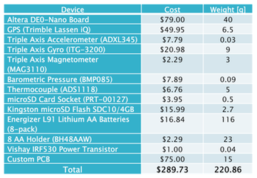
Overall this project is well within our weight specificationsod 1lb and budget of $400. The only part that has a flexible budget is the custom PCB fabrication. Depending on the feature sizes needed and the number many layers on the board itself, the price could be more expensive. $75 is a conservative amount.